Inside an optical module, where the watts and the dollars go
An 800G module that fits in your hand has a bill of materials over a thousand dollars and a power budget over ten watts. One chip inside it takes a third of the first and half of the second. That chip explains how the module economy works.
A small box with one job
Unplug an 800G transceiver from a switch. You hold a metal box smaller than a stick of butter. It costs on the order of a thousand dollars and draws about 14 watts. The hyperscalers buy tens of millions of them per year. The contents are worth knowing for a specific reason. This small box is where the copper-versus-optics asymmetry gets a physical answer. Its internal economics also decide much of the industry around it.
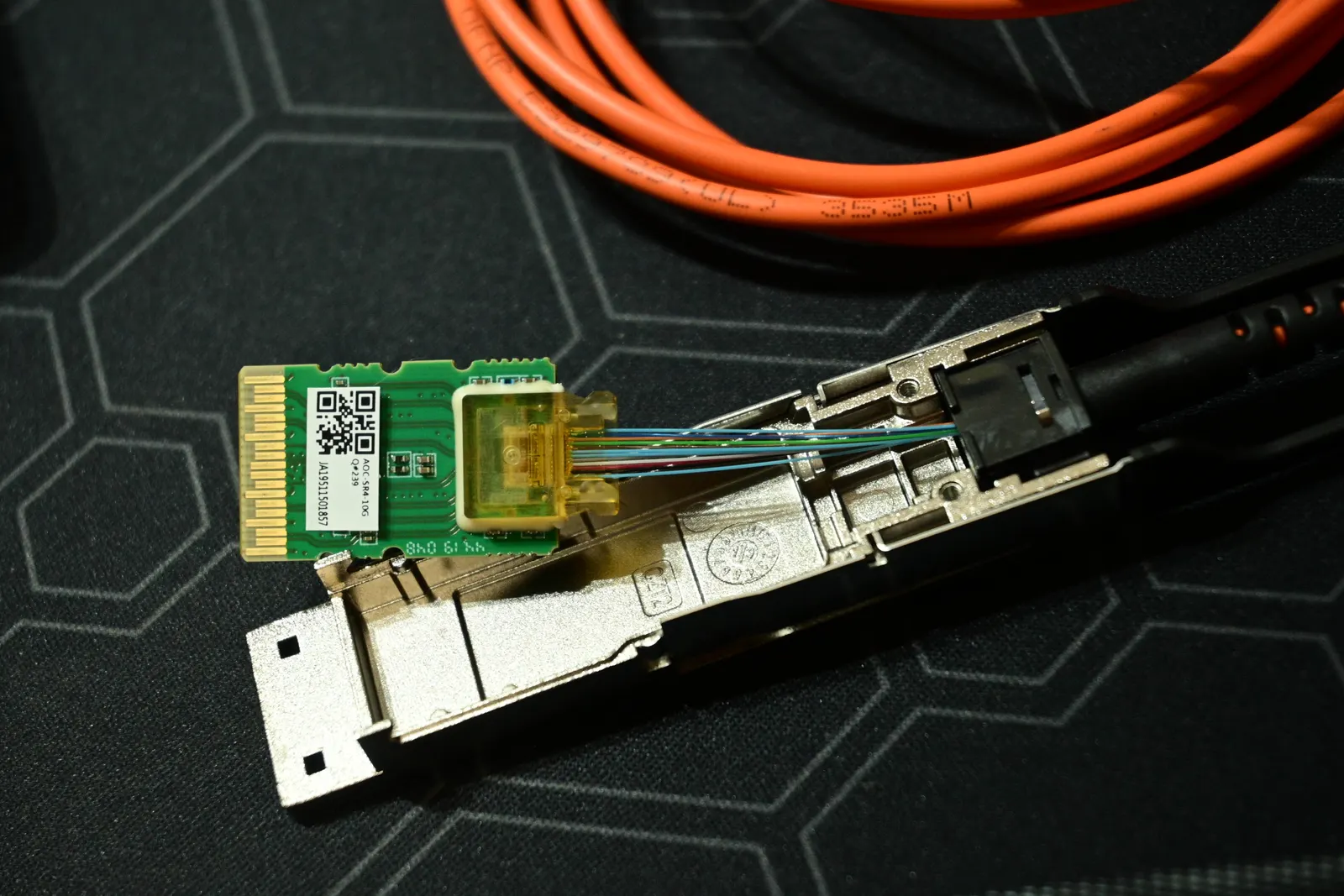
The box has exactly one job. It moves the boundary between two signaling methods. Electrical lanes come in through gold fingers, and light goes out through fiber. All the parts between them make that conversion work at 100 gigabits per lane:
Follow the signal from left to right:
- A DSP (digital signal processor) receives the degraded electrical lanes and retimes them into clean lanes.
- A driver takes the clean lanes and modulates a laser with enough swing.
- The light goes through an optical assembly, which is lenses and combiners aligned to sub-micron tolerances. Then it leaves the module.
- The receive path is the mirror image. It goes through a photodiode and a transimpedance amplifier (TIA), and then back through the same DSP.
A small management controller sits at the side. It reports temperature, bias current and optical power to the host over I²C.
Now add prices and power to the diagram. One component then takes most of it.
The chip that is the module
Start with cost. Published teardown work puts the DSP at 20 to 40 percent of an 800G module’s bill of materials. The most frequent value is near 30. The driver and TIA together take another 20-plus percent. All the other parts share the remainder: lasers, photodiodes, the precision optics, the board, the housing, the controller, and the assembly and test. We show that remainder as one bucket because no credible published split of it exists. Five invented percentages would look more precise but be less true.
Now power. The PAM4 DSP uses 6 to 8 watts, about half of the budget for the full module.
So one chip takes a third of the money and half of the heat. These costs are structural, not accidental. An optical DSP uses the same 7, 5 and now 3 nanometer processes as flagship phone silicon. But its volumes are orders of magnitude smaller, so each part carries a larger share of the mask-set cost. In economic terms, the module is a leading-edge logic chip in a metal sleeve, with high-precision optics attached.
The figure below shows all of these shares in one place:
Where the watts and the dollars go
One device, two budgets. The DSP dominates both, which is exactly why removing it is the industry's main lever on module power.
- Line rate
- 800G
- 8 × 100G
- DSP power
- 5.5 W
- 50% of the module
- Energy per bit
- 13.8 pJ
- the only cross-rate comparison
Power budget
- PAM4 DSP5.5 W50%
- Optics, driver, TIA, control5.5 W50%
Bill of materials
- PAM4 DSP30%
- Driver and TIA20%
- Everything elsenot separately published50%
- PAM4 DSP
- Quoted at 20–40% of an 800G bill of materials. Built on 7nm, 5nm and now 3nm at volumes orders of magnitude below consumer silicon, which is why it costs what it does.
- Driver and TIA
- Reported at over 20% between them, roughly evenly split.
- Everything else
- Lasers and photodiodes, the optical assembly and its alignment, the PCB, the housing and cage, the management controller, and assembly and test.
The number that went flat
The vendor datasheets contain the most honest single number in module engineering. One division shows it.
Broadcom’s 7nm platform enabled 400G modules at 7 watts and 800G modules at 14. Divide power by throughput. Both give exactly 17.5 picojoules per bit. A full product generation doubled the speed and added lanes. But the energy to move one bit did not improve at all. The module generation did not change this number. The silicon below it did. The 5nm DSP brought 800G to 11 watts, which is 13.75 pJ/bit. That is a 21 percent improvement, and all of it comes from the process node.
This fact changes the order of what matters. Module generations are packaging events. Efficiency generations are foundry events. So the energy path of optical interconnect follows the same leading-edge process roadmap as the rest of computing. It also has the same competition for foundry capacity. A concern about the power of future fabrics is, correctly, a question about how much more the DSP node can give.
The obvious surgery
If one chip uses half the power, the obvious step is to remove it. The industry tried this. Linear-drive pluggable optics (LPO) removes the DSP completely. High-linearity drivers and TIAs do as much equalization as they can. The SerDes of the host ASIC drives the optics almost directly. The reported result: an 800G module decreases from the 14-to-17 watt class to 7 to 8.5 watts. This cuts 17.5 pJ/bit to around 10.
This saving has a cost, and the cost is a split in responsibility. Without a DSP, the module does not correct the channel. The laser receives all the damage from the host trace and connectors, without correction. So the host SerDes and the board designer must carry that load. The length and quality of the electrical path decide if the trade is good. For this reason, LPO adoption follows switch platforms, not module catalogs. Also, as the asymmetry essay argues, LPO moves toward the short-reach NPO and CPO geometries. There, the host-side channel is too short to cause much damage.
Who makes each piece
Examine the layers of the box in order of buyer risk, highest first.
The DSP is the most concentrated layer. Marvell is widely reported as the share leader, and Broadcom is the main alternative. No analyst publishes the split. Credo and MaxLinear also offer 800G DSPs. Reports say that Marvell’s 3nm part cuts power by more than 20 percent against 5nm. After the flat line above, this is the type of improvement that counts. Here is the practical warning for buyers. Three qualified module vendors that all use the same DSP are one supplier with three badges.
Lasers are the second point of concentration. TrendForce counts two laser types together: EML (electro-absorption modulated laser) and CW-DFB (continuous-wave distributed-feedback laser). In that combined market, the top three suppliers hold about 55 percent:
- Broadcom
- Lumentum
- Sumitomo Electric
A long tail includes Coherent, Mitsubishi Electric, EMCORE, Accelink and others.
Capacity increases fast. Reports give combined EML and CW-DFB output of 50.7 million units a month in 2026. Convert both sides to the same units to make the figure useful. Published 2026 forecasts for 800G modules go from 33.5 to 49 million units. Forty million modules a year at eight lasers each is 320 million lasers, about 27 million a month. The highest forecast needs about 33 million a month. So the reported capacity covers the 800G demand, with margin for the larger laser count of 1.6T. That is supply checked against demand, not against a press release.
The CW (continuous-wave) half of that capacity is important for silicon photonics. A silicon photonic transmitter does not modulate its laser. It modulates light from a continuous-wave source. That source is a different part, and its supplier list is different from the EML supplier list.
The driver and TIA are moving into the DSP. Broadcom’s PHYs ship with both integrated, and this is one reason module power decreased. The management controller needs a name correction more than a market analysis. The part is a microcontroller with an analog front end. It does the digital diagnostic monitoring that SFF-8472 defines, under the CMIS framework at 400G and above. “AFE” is the name of a block inside that chip, not the chip. We found no credible supplier-share data for it, so this essay shows none.
The board is a real high-frequency component. It uses ultra-low-loss laminates with very-low-profile copper. Panasonic’s Megtron series is the reference, and Shengyi positions its S7439 as the equivalent. So the board is one of the few layers in the box with two real sources.
The housing and cage come from Amphenol, TE Connectivity and Molex. The form-factor choice is a thermal choice first. OSFP has a larger shell, which gives it more thermal margin as module power increases.
Assembly is the layer where China leads clearly:
- InnoLight has roughly 35 percent of 800G.
- Eoptolink is in the top five.
- Together the two hold about 60 percent of NVIDIA’s incremental orders.
- Other makers, Coherent among them, share the balance.
Where the volume actually is
Two deployment facts are easy to confuse, and both are true. First, the 800G generation carries the volume. It is in its mass-deployment years, and shipments still more than double. Second, 1.6T ramps on top of it, not after it. Volume shipments are in progress, and hyperscalers announced the first orders.
Nobody knows how steep that ramp will be. Published 2026 forecasts for 1.6T units go from five million to twenty. This four-fold spread mostly measures how little visibility anyone outside the hyperscalers’ order books has. We show the spread and do not pick a value, because the spread is the information.
The structural change is more important than either number. Optical generations used to ramp, level off and then give way to the next. Now 800G and 1.6T are both in volume production, and 3.2T parts are in validation. So every supplier in the chain must carry two generations of production and pay for a third at the same time. That is a working-capital problem as much as an engineering problem. It favors the large, concentrated suppliers that this article counted.
The moral of the box
The small box teaches a simple economic lesson in three parts:
- Its costs collect where the electrical-to-optical boundary is most difficult, which today means the DSP.
- Its efficiency moves only when the foundry node below it moves.
- Its suppliers concentrate at the two points where the physics is most difficult: retiming and lasing.
The boundary can move into near-package and co-packaged geometries. Then the box stops being a product category. But all of its functions and all of its suppliers continue, in new positions. So the box is worth understanding even if pluggables will not last forever. The module is temporary, but its anatomy is the anatomy of whatever replaces it.
What to take away
- A pluggable module moves a boundary, and its economics collect at that boundary. The DSP takes about 30 percent of the bill of materials and half the power.
- Energy per bit stayed flat across a module generation: 17.5 pJ/bit at both 400G and 800G on 7nm. It improved only with the 5nm node. Efficiency progress in optics is foundry progress.
- Linear drive removes the DSP and 40 to 50 percent of the power. It moves the cleanup load to the host. It fits best on short electrical paths, and these are more and more often NPO and CPO.
- Concentration is at the difficult physics: two vendors supply most of the DSPs. Three suppliers hold about 55 percent of the combined EML and CW-DFB laser market. Boards, housings and assembly are the layers with more than one source.
- Watch the 1.6T forecast spread, five to twenty million units for 2026. Read it as a measurement of opacity, not as a prediction. The box may be temporary, but its anatomy transfers to whatever comes next.